How to set track width by netclass in KiCad 10
A step-by-step tutorial on configuring netclasses in KiCad 10 so tracks like power nets automatically get a wider track width, using net name patterns.
A netclass in KiCad lets you group nets together and give them shared rules, such as clearance and track width. This is useful when a project needs wider tracks than the default, for example on power nets, which need to carry more current than a typical signal.
Creating a new netclass
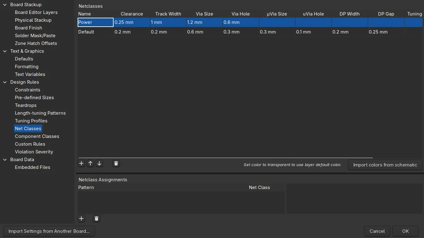
Open KiCad’s PCB editor and go to File => Board Setup.
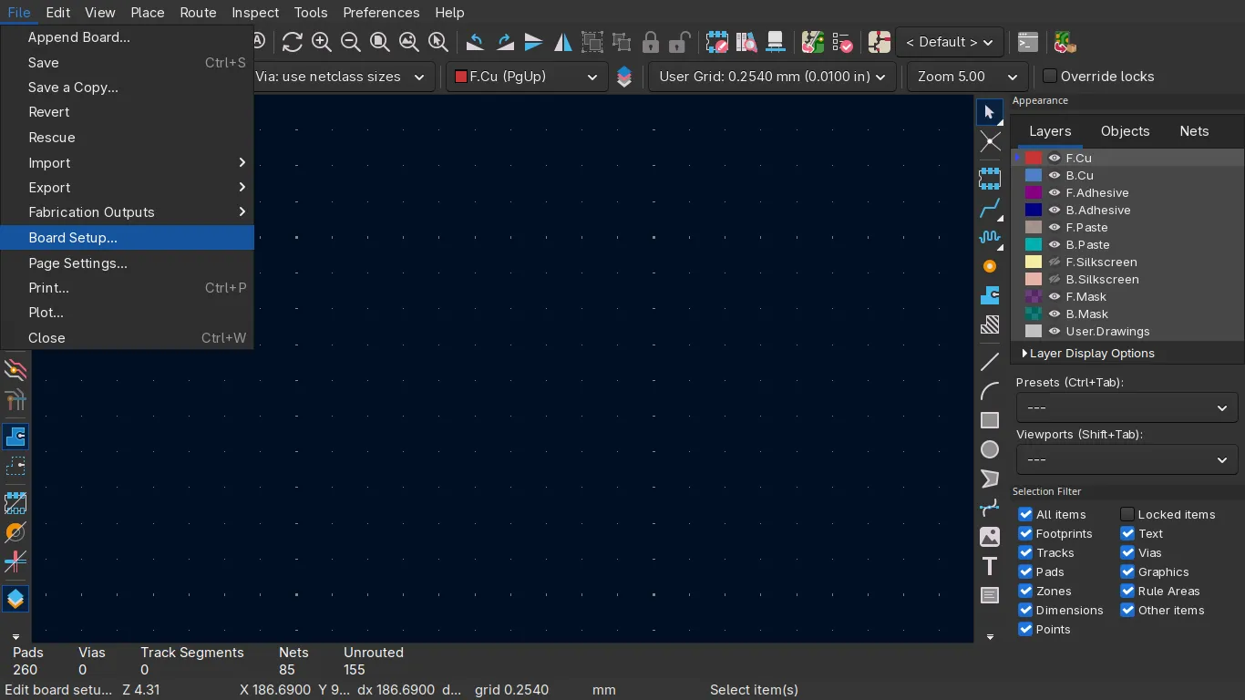
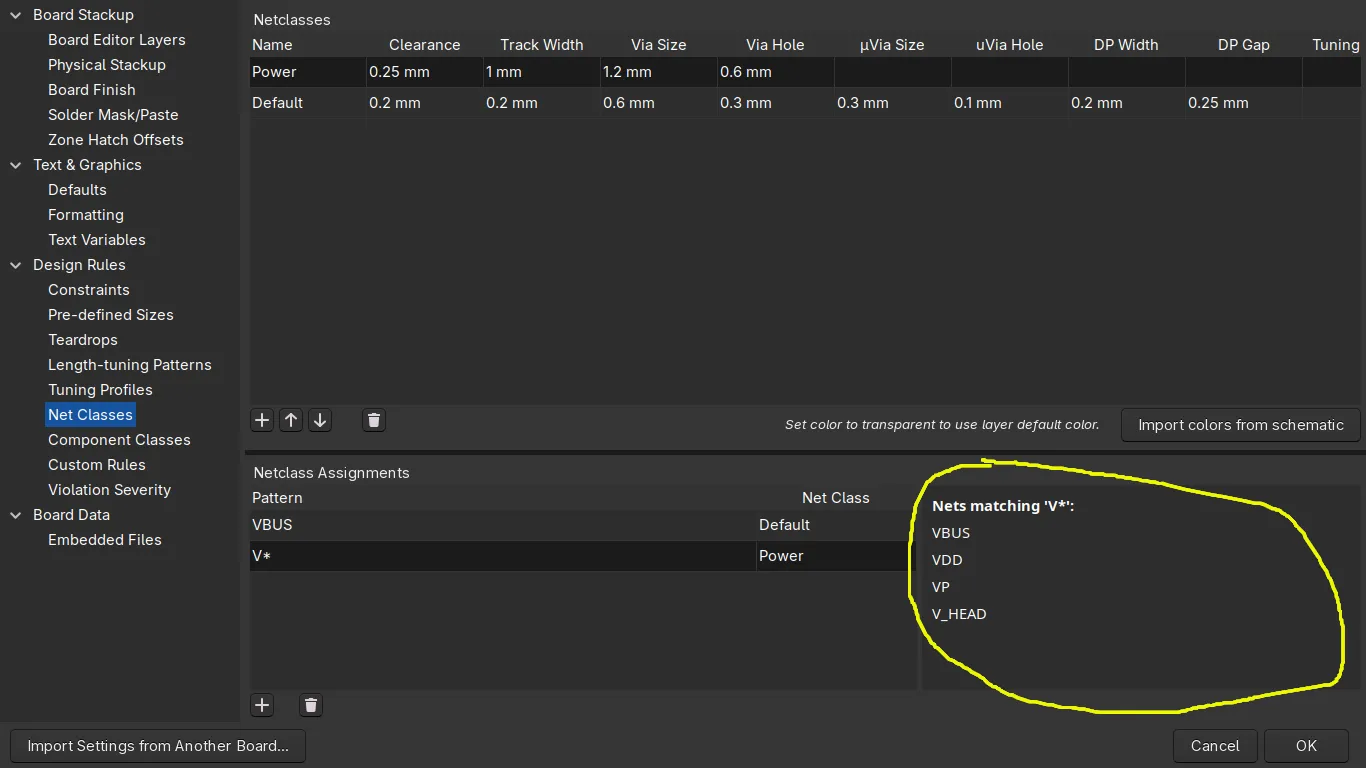
Then, under Open Design Rules, go to Net Classes. This opens the net class window.
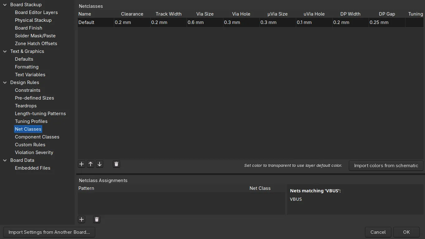
Create a new netclass by pressing the add button under the netclass list.
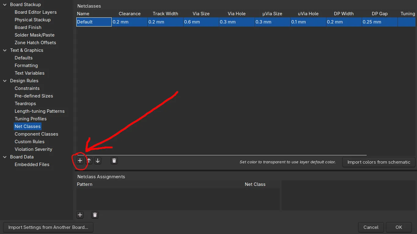
After creating it, fill out its values, such as name, clearance, track width, and others.
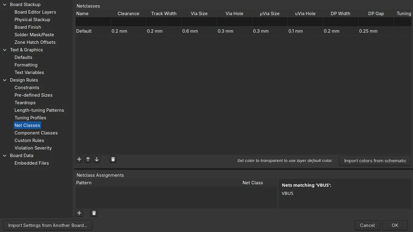
Creating a pattern to assign nets
With the netclass created, the next step is to set up a pattern. Patterns automatically match nets by name and assign them to a netclass.
To create a pattern, press the add button under the pattern list.
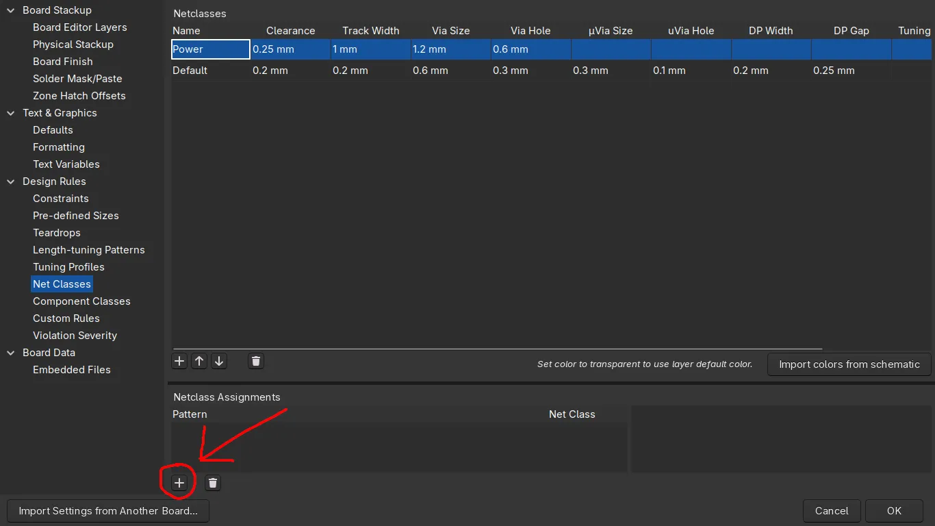
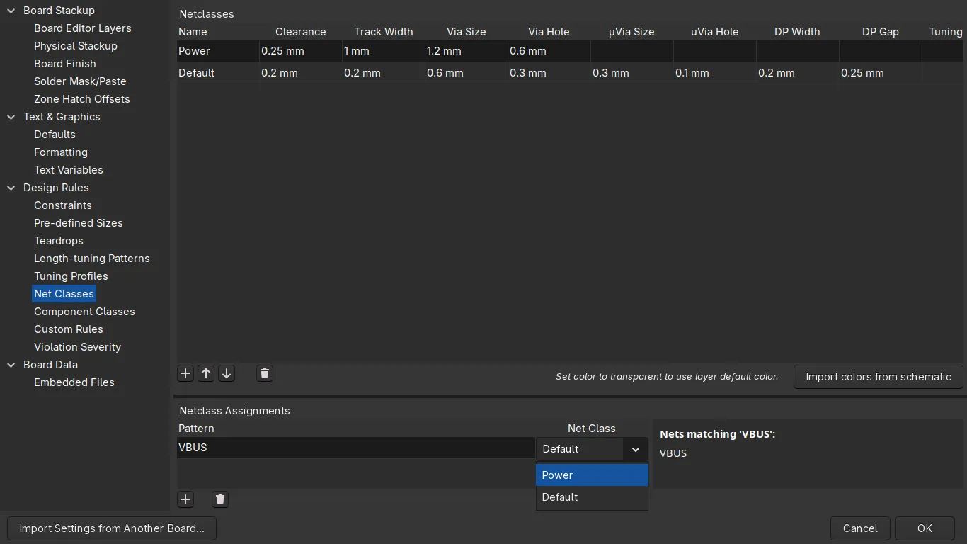
Set the pattern value (in my case, VBUS).
It’s also important to assign the pattern to the correct netclass, in my case the newly created Power netclass. This is done by selecting it from the drop-down next to the pattern.
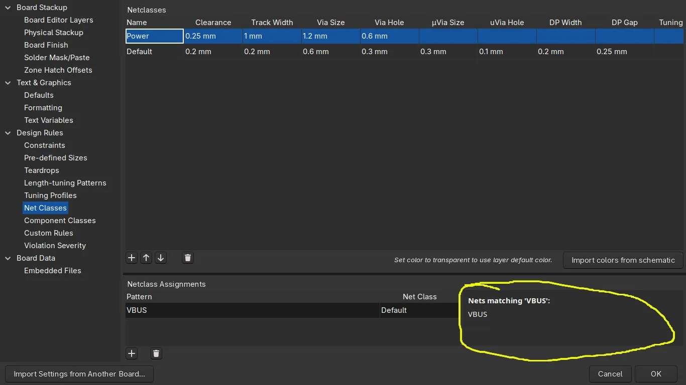
The pattern value also supports the wildcard * to match any characters. For example, VB* would achieve the same result, but would also match any other net starting with VB, such as VB1.
The bottom-right window shows which nets currently match the pattern.
Here’s an example using the pattern V*, which matches all of my nets VBUS, VDD, VP, and V_HEAD, assigning them all to the Power netclass.
Everything is now set up. Close the Board Setup window by pressing OK.
Result
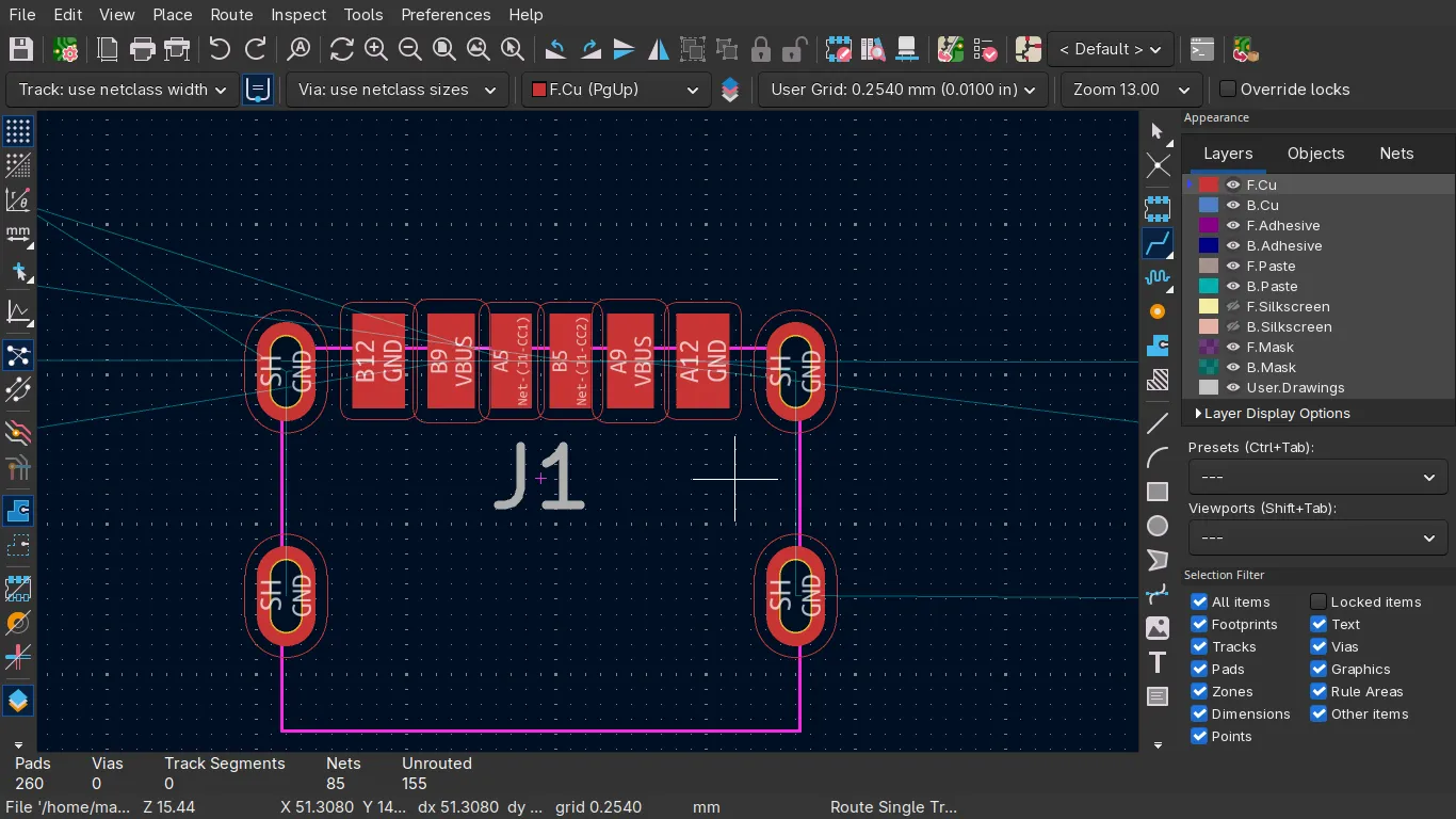
Here’s a USB connector, where one of the pads is on the VBUS net, which I’ve assigned to the power netclass.
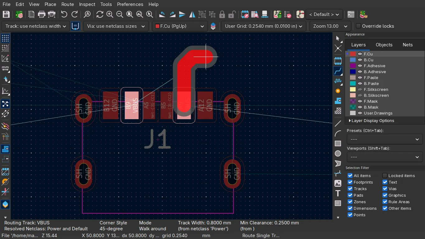
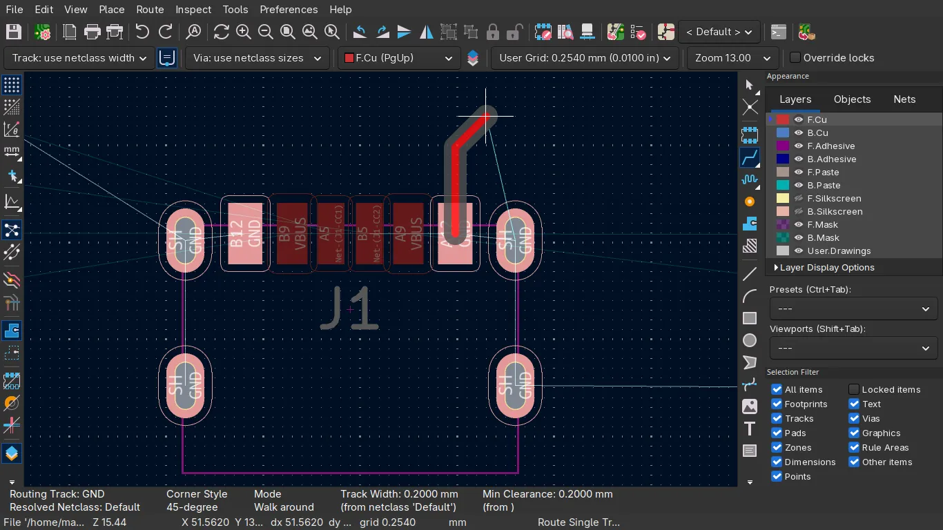
Creating a track from VBUS now automatically uses the wider track width, while other pads still use the default netclass.
Conclusion
Netclasses with pattern matching make it easy to keep power (or any other) nets routed at a consistent, wider width without manually setting the track size every time. Once the pattern is set up, KiCad handles it automatically for any matching net.