Gowin IDE Tutorial: Button Input
Learn how to use a button as a digital input in Verilog and control an LED using Gowin IDE on the Sipeed Tang Primer 20K FPGA development board.
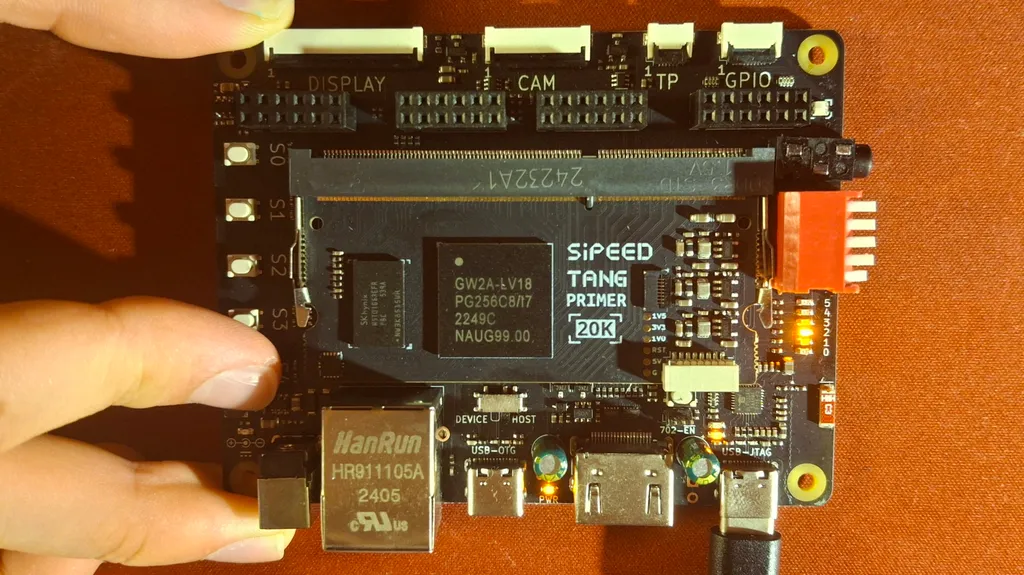
The LED turns on while the button is being pressed.
The only prerequisite is knowing how to create a new Gowin project and a Verilog source file. These steps were covered in the first tutorial.
I am again using the Tang Primer 20K Dock with the GW2A-LV18PG256C8/I7 FPGA.
Create a new Gowin project for your board and add a new Verilog file. I named mine top.v.
About
This is a very simple example of reading a push button.
While the button is pressed, the LED will be turned on. When the button is released, the LED will turn off.
In a later tutorial, we will make the button toggle the LED instead. In that case, pressing the button once will turn the LED on and pressing it again will turn it off.
Writing the Verilog
The complete Verilog code is very small:
module top(
    input buttonInput,
    output led
);

    assign led = buttonInput;
endmodule
Let’s look at what the code does.
First, we create a module called top with two ports:
module top(
    input buttonInput,
    output led
);

endmodulebuttonInputis an input connected to the physical push button on the board.ledis an output connected to the physical LED.
The following line continuously assigns the value of buttonInput to led:
assign led = buttonInput;This means that when buttonInput is logic 1, led will also be logic 1. When buttonInput changes, the LED output changes with it.
On the Tang Primer 20K Dock, both the push button and LED are active-low. Pressing the button produces logic 0, and the LED turns on when its output is logic 0. Because they use the same polarity, we can connect them directly with assign led = buttonInput;.
Unlike the blinking LED example from the previous tutorial, there is no clock, counter, or other sequential logic here. This is simple combinational logic: the output directly depends on the current value of the input.
Pin Assignment
After writing the Verilog, run Synthesize.
Once synthesis finishes successfully, open FloorPlanner. The default I/O constraints should now look like:

LED
For my Tang Primer 20K Dock, the LED uses the following constraints:
Location: N16
I/O Type: LVCMOS33
Pull Mode: None

Button
For my board revision, I am using one of the user buttons, marked S4 on my board:
Location: C7 (*Note below)
I/O Type: LVCMOS15 (*Note below)
Pull Mode: None
PCI Clamp: Off

The complete Physical Constraints File looks like this:
IO_LOC "led" N16;
IO_PORT "led" IO_TYPE=LVCMOS33 PULL_MODE=NONE DRIVE=8 BANK_VCCIO=3.3;

IO_LOC "buttonInput" C7;
IO_PORT "buttonInput" IO_TYPE=LVCMOS15 PULL_MODE=NONE PCI_CLAMP=OFF BANK_VCCIO=1.5;The Tang Primer 20K Dock has multiple hardware revisions, and the button connections have changed between rev. 3713 and rev. 3714.
Revision 3713 (2023) (I have this one)
- Button:
S4 - FPGA pin:
C7 - I/O type:
LVCMOS15
Revision 3714 (2026)
S4is connected to FPGA pinB10B10is also the FPGA’sRECONFIG_N/RECFGconfiguration pin- Because this pin has a special FPGA configuration function, do not use
S4as the input button - Instead, use one of the other user buttons and assign the corresponding FPGA pin from the rev. 3714 schematic
Make sure you check which board revision you have before copying the pin constraints.
Programming and Testing
Save the constraints and run Place & Route.
After Place & Route finishes successfully, open Programmer and upload the design to the FPGA.
Preview
After programming the FPGA, pressing the button should turn the LED on. Releasing the button should turn the LED off.
Here is the finished result: